Edge Triggered Flip Flop Circuit Diagram
Flip edge triggered flop positive flops computer engineering state lecture machines monday week ppt powerpoint presentation Edge-triggered d flip-flop behavior Jk flipflop edge triggered negative example projects flipflops examples
STORAGE ELEMENTS : FLIP FLOPS - Gate CSE - UPSCFEVER
Flip flop edge positive trigger level schematic using circuit type instead why circuitlab created stack logic Negative edge triggered d flip flop circuit diagram Digital logic
Sr flip flop diagram edge timing positive triggered solved help waveform given please complete
Flop flip triggered positive sponsored mikroraFlip flop triggered circuit flops electronics Digital logicFlop flip edge triggered circuit circuits simulation simulator.
Flip flop edge triggered circuit nand positive input logic type gates circuits create there clock coupled cross electronics flipflop schematicFlip flop edge triggered circuit trigger logic digital approach negative using gates stack Rs flip flop diagramSolved question 1 referring to the positive-edge triggered d.

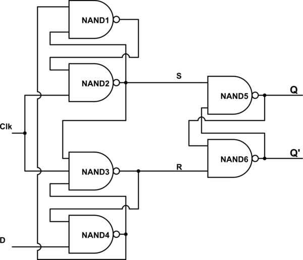
Digital logic
Storage elements : flip flopsFlip edge triggered flops flop positive symbol clock inputs note ppt powerpoint presentation input Negative edge triggered d flip flop circuit diagramFlop flip triggered circuit nand implementation.
Solved for a positive-edge-triggered d flip-flop with inputsFlip flop edge triggered behavior Negative flop triggered chegg convertTriggered flop slave.

Flop flip cmos implementation using triggered edge diagram logic circuit implement provides trying wikipedia following am search google
Solved given a positive edge triggered sr flip-flop,Negative edge triggered d flip flop circuit diagram Edge flip flop timing triggered diagram negativeCircuit design.
Timing diagram for a negative edge triggered flip flopFlip flop circuit diagram edge triggered block sequential blocks unit building upscfever truth table flops elements storage logical organization computer Flip flop edge triggered positive timing jk diagram output inputs shown digital logic sketch clk below question solvedEdge-triggered d flip-flop.


PPT - ELEC1700 Computer Engineering 1 Week 9 Monday lecture Flip-flops

STORAGE ELEMENTS : FLIP FLOPS - Gate CSE - UPSCFEVER
digital logic - Why is D Flip Flop Positive Edge Trigger instead of a

Negative Edge Triggered D Flip Flop Circuit Diagram - vayp-por

digital logic - Is there an intuitive explanation of the classic edge

Edge-Triggered D Flip-Flop - Online Circuit Simulator

Timing Diagram for A Negative Edge Triggered Flip Flop - YouTube

Solved Given a positive edge triggered SR flip-flop, | Chegg.com

Solved For a positive-edge-triggered D flip-flop with inputs | Chegg.com